- 您现在的位置:买卖IC网 > Sheet目录17378 > ADP2105-1.8-EVALZ (Analog Devices Inc)BOARD EVALUATION ADP2105Z 1.8V
�� �
�
�Data� Sheet�
�ADP2105/ADP2106/ADP2107�
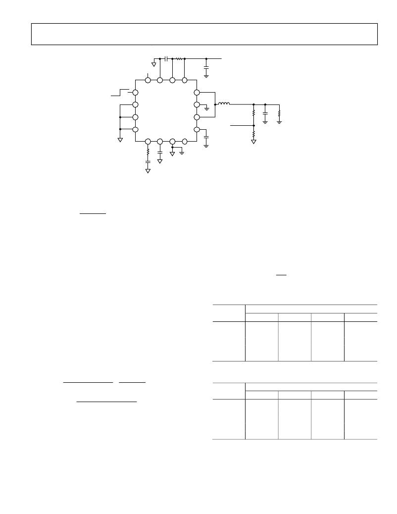
�0.1μF�
�1� 0Ω�
�V� IN�
�INPUT� VOLTAGE� =� 2.7V� TO� 5.5V�
�C� IN1�
�FB�
�16�
�15�
�14�
�13�
�OFF�
�ON�
�1�
�EN�
�FB�
�GND�
�IN�
�PWIN1�
�LX2� 12�
�2�
�3�
�4�
�GND�
�GND�
�GND�
�ADP2105/�
�ADP2106/�
�ADP2107�
�PGND� 11�
�LX1� 10�
�PWIN2� 9�
�V� IN�
�L�
�FB�
�R� TOP�
�OUTPUT� VOLTAGE�
�=� 0.8V� TO� V� IN�
�C� OUT�
�LOAD�
�COMP�
�5�
�SS�
�6�
�AGND� NC�
�7�
�8�
�C� IN2�
�R� BOT�
�R� COMP�
�C� SS�
�C� COMP�
�NC� =� NO� CONNECT�
�Figure� 38.� Typical� Applications� Circuit� for� Adjustable� Output� Voltage� Option� of� ADP2105/ADP2106/ADP2107(ADJ)�
�R� TOP� =� R� BOT� ?� OUT�
�I� PK� =� I� LOAD� (� MAX� )� +� ?�
�?� ?� I� L� ?�
�?� 2� ?�
�?� I� L� =� OUT�
�V� � (� V� IN� ?� V� OUT� )� I� LOAD� (� MAX� )�
�When� R� BOT� is� determined,� calculate� the� value� of� the� top� resistor�
�(� R� TOP� )� by� using� the� following� equation:�
�?� V� ?� V� FB� ?�
�?�
�?� V� FB� ?�
�The� ADP2105/ADP2106/ADP2107(x.x� V)� include� the� resistive�
�voltage� divider� internally,� reducing� the� external� circuitry� required.�
�For� improved� load� regulation,� connect� the� FB� to� the� output�
�voltage� as� close� as� possible� to� the� load.�
�INDUCTOR� SELECTION�
�The� high� switching� frequency� of� ADP2105/ADP2106/ADP2107�
�allows� for� minimal� output� voltage� ripple� even� with� small� inductors.�
�The� sizing� of� the� inductor� is� a� trade-off� between� efficiency� and�
�transient� response.� A� small� inductor� leads� to� larger� inductor�
�current� ripple� that� provides� excellent� transient� response� but�
�degrades� efficiency.� Due� to� the� high� switching� frequency� of�
�ADP2105/ADP2106/ADP2107,� shielded� ferrite� core� inductors�
�are� recommended� for� their� low� core� losses� and� low� electromagnetic�
�interference� (EMI).�
�As� a� guideline,� the� inductor� peak-to-peak� current� ripple� (ΔI� L� )� is�
�typically� set� to� 1/3� of� the� maximum� load� current� for� optimal�
�transient� response� and� efficiency,� as� shown� in� the� following�
�equations:�
�≈�
�V� IN� � f� SW� � L� 3�
�For� the� ADP2106�
�L� >� (0.83� μH/V)� ×� V� OUT�
�For� the� ADP2107�
�L� >� (0.66� μH/V)� ×� V� OUT�
�Inductors� 4.7� μH� or� larger� are� not� recommended� because� they�
�may� cause� instability� in� discontinuous� conduction� mode� under�
�light� load� conditions.� It� is� also� important� that� the� inductor� be�
�capable� of� handling� the� maximum� peak� inductor� current� (I� PK� )�
�determined� by� the� following� equation:�
�?�
�Table� 6.� Minimum� Inductor� Value� for� Common� Output�
�Voltage� Options� for� the� ADP2105� (1� A)�
�V� IN�
�V� OUT� 2.7� V� 3.6� V� 4.2� V� 5.5� V�
�1.2� V� 1.67� μH� 2.00� μH� 2.14� μH� 2.35� μH�
�1.5� V� 1.68� μH� 2.19� μH� 2.41� μH� 2.73� μH�
�1.8� V� 2.02� μH� 2.25� μH� 2.57� μH� 3.03� μH�
�2.5� V� 2.80� μH� 2.80� μH� 2.80� μH� 3.41� μH�
�3.3� V� 3.70� μH� 3.70� μH� 3.70� μH� 3.70� μH�
�Table� 7.� Minimum� Inductor� Value� for� Common� Output�
�Voltage� Options� for� the� ADP2106� (1.5� A)�
�V� IN�
�2� .� 5� � V� OUT� � (� V� IN� ?� V� OUT� )�
�V� IN� � I� LOAD� (� MAX� )�
�?� L� IDEAL� =� μ� H�
�where� f� SW� is� the� switching� frequency� (1.2� MHz).�
�The� ADP2105/ADP2106/ADP2107� use� slope� compensation� in�
�the� current� control� loop� to� prevent� subharmonic� oscillations�
�V� OUT�
�1.2� V�
�1.5� V�
�1.8� V�
�2.5� V�
�3.3� V�
�2.7� V�
�1.11� μH�
�1.25� μH�
�1.49� μH�
�2.08� μH�
�2.74� μH�
�3.6� V�
�2.33� μH�
�1.46� μH�
�1.50� μH�
�2.08� μH�
�2.74� μH�
�4.2� V�
�2.43� μH�
�1.61� μH�
�1.71� μH�
�2.08� μH�
�2.74� μH�
�5.5� V�
�1.56� μH�
�1.82� μH�
�2.02� μH�
�2.27� μH�
�2.74� μH�
�when� operating� beyond� 50%� duty� cycle.� The� fixed� slope� compen-�
�sation� limits� the� minimum� inductor� value� as� a� function� of�
�output� voltage.�
�For� the� ADP2105�
�L� >� (1.12� μH/V)� ×� V� OUT�
�Rev.� D� |� Page� 17� of� 36�
�发布紧急采购,3分钟左右您将得到回复。
相关PDF资料
ECM10DCMN-S288
CONN EDGECARD 20POS .156 EXTEND
ADP2102-4-EVALZ
BOARD EVAL 2.5V-3.3V ADJ OUTPUT
ADP2102-3-EVALZ
BOARD EVAL 1.5V-1.875V ADJ OUTPT
195D685X9020X2T
CAP TANT 6.8UF 20V 10% 2910
195D685X0020X2T
CAP TANT 6.8UF 20V 20% 2910
R1S-1524/H-R
CONV DC/DC 1W 15VIN 24VOUT
195D226X0004X2T
CAP TANT 22UF 4V 20% 2910
A9CAG-0303F
FLEX CABLE - AFG03G/AF03/AFE03T
相关代理商/技术参数
ADP2105ACPZ
制造商:Analog Devices 功能描述:V REG 1A ADJ SMD LFCSP-16 2105
ADP2105ACPZ-1.2-R7
功能描述:IC REG BUCK SYNC 1.2V 1A 16LFCSP RoHS:是 类别:集成电路 (IC) >> PMIC - 稳压器 - DC DC 开关稳压器 系列:- 标准包装:500 系列:- 类型:切换式电容器(充电泵),反相 输出类型:固定 输出数:1 输出电压:-3V 输入电压:2.3 V ~ 5.5 V PWM 型:Burst Mode? 频率 - 开关:900kHz 电流 - 输出:100mA 同步整流器:无 工作温度:-40°C ~ 85°C 安装类型:表面贴装 封装/外壳:SOT-23-6 细型,TSOT-23-6 包装:带卷 (TR) 供应商设备封装:TSOT-23-6 其它名称:LTC1983ES6-3#TRMTR
ADP2105ACPZ-1.5
制造商:Analog Devices 功能描述:V REG 1A 1.5V SMD LFCSP-16 2105
ADP2105ACPZ-1.5-R7
功能描述:IC REG BUCK SYNC 1.5V 1A 16LFCSP RoHS:是 类别:集成电路 (IC) >> PMIC - 稳压器 - DC DC 开关稳压器 系列:- 标准包装:500 系列:- 类型:切换式电容器(充电泵),反相 输出类型:固定 输出数:1 输出电压:-3V 输入电压:2.3 V ~ 5.5 V PWM 型:Burst Mode? 频率 - 开关:900kHz 电流 - 输出:100mA 同步整流器:无 工作温度:-40°C ~ 85°C 安装类型:表面贴装 封装/外壳:SOT-23-6 细型,TSOT-23-6 包装:带卷 (TR) 供应商设备封装:TSOT-23-6 其它名称:LTC1983ES6-3#TRMTR
ADP2105ACPZ-1.8
制造商:Analog Devices 功能描述:V REG 1A 1.8V SMD LFCSP-16 2105
ADP2105ACPZ-1.8-R7
功能描述:IC REG BUCK SYNC 1.8V 1A 16LFCSP RoHS:是 类别:集成电路 (IC) >> PMIC - 稳压器 - DC DC 开关稳压器 系列:- 产品培训模块:Lead (SnPb) Finish for COTS
Obsolescence Mitigation Program 标准包装:50 系列:- 类型:升压(升压) 输出类型:两者兼有 输出数:1 输出电压:5V,2 V ~ 16.5 V 输入电压:2 V ~ 16.5 V PWM 型:- 频率 - 开关:45kHz 电流 - 输出:50mA 同步整流器:无 工作温度:0°C ~ 70°C 安装类型:通孔 封装/外壳:8-DIP(0.300",7.62mm) 包装:管件 供应商设备封装:8-PDIP
ADP2105ACPZ-3.3
制造商:Analog Devices 功能描述:V REG 1A 3.3V SMD LFCSP-16 2105
ADP2105ACPZ-3.3R7
制造商:Rochester Electronics LLC 功能描述: 制造商:Analog Devices 功能描述: